Rolling Mask Lithography – RML®
Rolling Mask Lithography (RML®) is our patented manufacturing technology that offers a unique advantage in the smart materials industry. RML® employs a massively parallel patterning scheme that is easily scalable to large areas of rigid substrate materials (plates and panels) and rolls of flexible films. Its nano-fabrication method combines the advantages of Soft Lithography and Near-field Optical Lithography, proved to be reliable in fabrication of nano-structures beyond the diffraction limit.
Our RML technology is used to produce certain types of smart materials made from a variety of substrates including glass, metal semiconductors, and polymer films. As a result, we are able to block, absorb or enhance light and other forms of energy. Our method uses near-field phase shift photolithography which can be implemented as a continuous, seamless and scalable manufacturing process. RML can be used to manufacture smart materials in a variety of shapes and sizes. With RML technology, we are creating a new generation of optical metamaterials that satisfy commercial requirements for nano-structured surfaces with large area and low cost. It is compatible with roll-to-plate and roll-to-roll process modes. RML is free from form-factor limitations associated with state-of-the-art projection optical lithography (steppers), pattern type limitations of holographic and self-assembly lithography methods, and process integration and yield limitations of nano-imprint lithography.
RML’s versatility is advancing our smart material research and helping to produce new metamaterial solutions that span from medical imaging systems to automotive, communications and consumer electronics applications, to satellites orbiting the Earth.
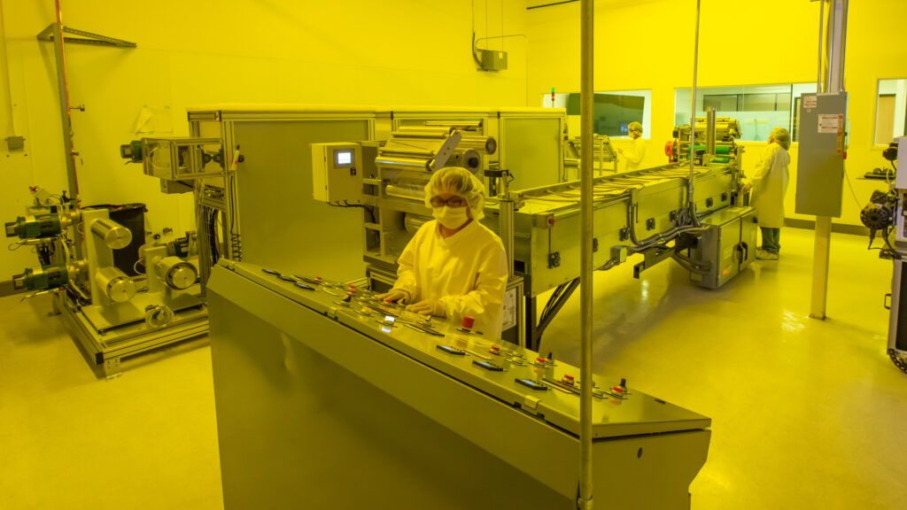
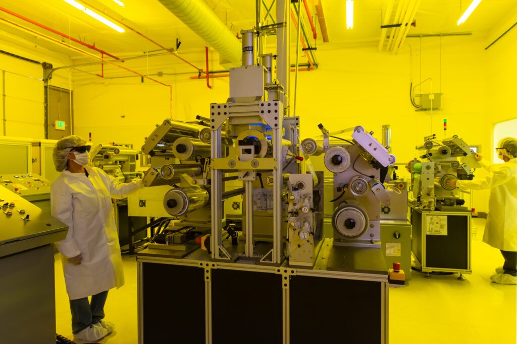
META’s Pilot Scale RML Line in Pleasanton, California
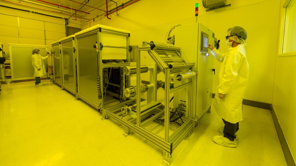
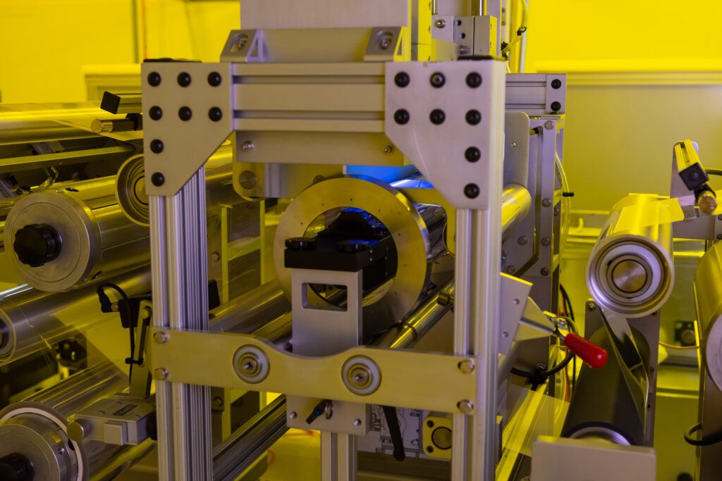
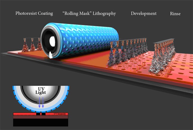
The RML pilot scale roll-to-roll system pictured below, a first of its kind in metamaterials, processes 300mm wide flexible substrates. In subsequent generations, META intends to scale the web width to 500mm and 1 meter or more, increasing capacity and reducing cost per square meter. Substrates are pre-coated with photoresist. The RML exposure step transfers a pattern to the photoresist.
How does RML® produce metamaterials and functional surfaces?
In order to alter how light interacts with structured materials, we use in-house computer software to engineer patterned nano-structures. It is modelled, optimized, and then transferred onto a soft cylindrical photomask. The RML uses the mask to pattern photosensitive materials deposited on a surface such as a glass plate or plastic thin film. Then patterns are used as etch masks for subsequent etching of a substrate (glass, semiconductor), or as templates for nano-structuring metals or other functional materials. In order to create a desired pattern on the surface, the RML equipment uses ultraviolet (UV) illumination as the mask rolls across the photosensitive film. We use RML due to its unique capability to create nano-structures within metamaterial films that are as small as 175 nanometers. Depending on the type of smart material being produced, our engineers add more layers to the film to increase its functionality.
As RML is an optical lithography method, it allows fabrication of both positive and negative nanopatterns from the same mask. RML also does not have a “nanoimprint residual layer”, which makes process integration (substrate etch or photoresist lift-off) much easier.
RML Further Process Steps
After RML exposure, the substrate is baked to stabilize the printed design, development creates 3D structures in the photoresist, metallization fills the 3D pattern to create a continuous metal mesh, and lift off removes the residual metal and photoresist.